Notes for Week 14
← back to syllabus ← back to notes
Topics
- CPU interrupts and exceptions
- Basics of memory caching for CPUs
- Intro to virtual memory
Introduction to Exceptions and Interrupts
- Exceptions and interrupts are unexpected events that require a change in the flow of control during program execution.
- While different instruction set architectures (ISAs) may use the terms differently, in MIPS terminology:
- An Interrupt is an exception that comes from outside the processor, typically from an external I/O controller or device request.
- An Exception arises from within the CPU itself. This can be due to events like an undefined opcode, arithmetic overflow, or executing a system call instruction.
- Hardware malfunctions can also cause either exceptions or interrupts.
- Handling these events without sacrificing performance is difficult.
Causes and Types of Exceptions and Interrupts in MIPS
Common events that trigger exceptions or interrupts in MIPS include:
- I/O device request (Interrupt). These are usually maskable, meaning they can be temporarily ignored if interrupts are disabled.
- Invoke the operating system from a user program (Exception). This is typically done using a special instruction like
syscall.
- Arithmetic overflow (Exception). MIPS can trap on overflow.
- Using an undefined instruction (Exception).
- Hardware malfunctions (Either Exception or Interrupt).
- Division by zero.
- Attempts to read nonexistent memory.
- Debugger breakpoints.
- Page faults or TLB misses which occur during memory access.
- External interrupts received on dedicated pins like INTR (maskable) or NMI (nonmaskable). Nonmaskable interrupts cannot be prevented.
MIPS Exception and Interrupt Handling Process
When an exception or interrupt occurs and is recognized by the processor, a sequence of events takes place:
- Detection: The processor detects the exceptional condition or receives an interrupt signal. Processors often check for interrupts after completing the execution of the current instruction.
- Finish Current Instruction (usually): For interrupts, the processor typically finishes the execution of the current instruction before responding. Pipelined processors may need to handle this differently, potentially involving flushing instructions in the pipeline.
- Save Processor State: The processor needs to save enough information to resume the interrupted program later.
- The address of the offending or interrupted instruction is saved in a special register called the Exception Program Counter (EPC). This is analogous to using the $ra register for saving the return address during a jump-and-link (
jal) instruction.
- The cause of the exception is recorded in another special register called the Cause register. The exception handler routine reads this register to determine how to proceed. MIPS uses different codes in the Cause register for different events.
- Other status information, such as the Program Status Word (PSW) or processor status register (PS), may also be saved, sometimes automatically in a dedicated register (like IPS in some architectures) or on the system stack.
- In MIPS, the EPC and Cause registers, along with others used for system functions, are typically part of Coprocessor 0 (CP0).
- Transfer Control to Handler: The processor transfers execution control to a predefined address where the exception handler or interrupt service routine (ISR) resides.
- The starting address of the routine is loaded into the Program Counter (PC).
- Many MIPS implementations use a single fixed entry point address for all exceptions (e.g., 8000 0180hex or 8000 0000hex for TLB misses). The handler code at this address then uses the Cause register to determine the specific event and branch to the appropriate specific handler code. Alternatively, some architectures (or MIPS implementations) might use vectored exceptions, where each exception type jumps directly to a different handler address.
- The processor may switch from user mode to supervisor mode (or kernel mode). This is necessary for the OS handler to access privileged resources and instructions.
- Execute the Handler Routine: The handler routine performs the actions necessary to deal with the exception or interrupt.
- Software can access the EPC and Cause registers using the
mfc0 (move from coprocessor 0) instruction, copying their contents into a general-purpose register. Similarly, mtc0 (move to coprocessor 0) can be used to write to these registers.
- The handler should save any general-purpose registers it might modify if they were not automatically saved, often on the system stack.
- If exceptions were automatically disabled upon entering the handler (to prevent nested exceptions), they must be re-enabled at an appropriate point in the handler, usually after saving necessary state. Disabling/enabling is often controlled by a bit in the processor status register and can be managed using instructions like
ei (enable interrupts) and di (disable interrupts).
- Return to Interrupted Program: After handling the event, the processor needs to return to the point where the original program was interrupted.
- In MIPS, this is done using the
ERET (Return from Exception) instruction. This instruction also typically resets the processor back to user mode.
- The
ERET instruction transfers control to the address stored in the EPC.
- For some exceptions like TLB misses or page faults, the instruction that caused the exception is re-executed after the handler has resolved the issue. This requires that the instruction be restartable, meaning its execution can be resumed after an exception without affecting the result.
Integration with Instruction Cycle and Pipelining
- Exceptions and interrupts interact with the fundamental instruction cycle (fetch-decode-execute). Checking for interrupts is often done as part of or after the execute cycle.
- In pipelined processors, handling exceptions and interrupts becomes more complex. When an exception occurs in a pipeline stage, instructions behind it in the pipeline must be prevented from completing, and instructions ahead of it need to be flushed (discarded), often by turning them into no-operation (nop) instructions.
- Achieving precise exceptions (where all instructions before the interrupting one complete, and no instructions after it complete) may require stalling the pipeline.
- When multiple exceptions occur simultaneously in different pipeline stages, the hardware typically prioritizes them so that the exception from the earliest instruction is serviced first.
- The Cause register records all pending exceptions that occurred in a clock cycle, and exception software uses this information along with the knowledge of which pipeline stage different exception types are detected in to correctly identify and handle the cause. For example, an undefined instruction is detected in the decode (ID) stage, while an arithmetic overflow might be detected in the execute (EX) stage.
Role of the Operating System
- The operating system (OS) software plays a crucial role in handling exceptions and interrupts.
- The OS uses exceptions to communicate with and control the execution of user programs (e.g., via
syscall).
- Hardware interrupts are used by the OS to manage I/O operations.
- The OS exception handler needs to run in a privileged mode (supervisor mode) to manage system resources and state, including special registers like EPC and Cause, which it accesses using
mfc0/mtc0.
- Memory management tasks like handling TLB misses and page faults are often implemented in OS software routines that are invoked via the exception mechanism.
MIPS Exception Worked Example
Here is a conceptual worked example illustrating how MIPS handles an arithmetic overflow exception in a pipelined processor.
Handling an Arithmetic Overflow Exception in MIPS
This example focuses on the events that occur when an add instruction triggers an arithmetic overflow in a pipeline MIPS processor.
Scenario:
Imagine the following sequence of MIPS instructions being executed in a pipelined processor:
        ...         # Instructions before the potential overflow
0x40:  sub $11, $2, $4
0x44:  and $12, $2, $5
0x48:  or $13, $2, $6
0x4C:  add $1, $2, $1   # Assume the sum of $2 and $1 exceeds the maximum
                        # representable signed 32-bit integer, causing overflow.
0x50:  slt $15, $6, $7
0x54:  lw  $16, 50($7)
        ...         # Subsequent instructions
Assume the processor is executing these instructions concurrently in its pipeline stages, i.e., Instruction Fetch (IF), Instruction Decode (ID), Instruction Execute (EX), Memory Access (MEM), register Write-back (WB).
Process When Overflow Occurs:
- Instruction Execution & Detection (EX Stage): The
add $1, $2, $1 instruction at address 0x4C reaches the Execute (EX) stage of the pipeline. During its operation in the ALU, the arithmetic overflow condition is detected. Note, the MIPS instructions add, addi, and sub are designed to cause exceptions on overflow. (see the MIPS ISA Green Sheet notes for each instruction)
- Initiating Exception Handling (Hardware Actions): Upon detecting the overflow, the hardware initiates the exception handling process. This is treated similarly to a control hazard in the pipeline.
- Save Program Counter: The address of the instruction that caused the exception is saved in a special register called the Exception Program Counter (EPC). MIPS typically saves the address of the next, following instruction (PC + 4) in the EPC. So, in this case, 0x50 (0x4C + 4) is saved in the EPC.
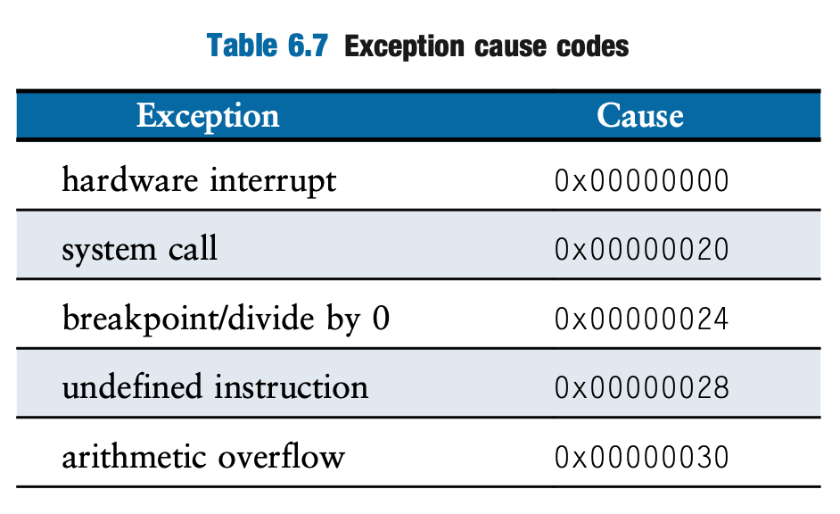
- Record Exception Cause: The hardware records the reason for the exception (arithmetic overflow) in the Cause register. See Table 6.7, which indicates the code for arithmetic overflow is 0x00000030. The Cause register can potentially record multiple pending exceptions that occur in the same clock cycle, allowing the exception software to prioritize.
- Flush Pipeline: Instructions that entered the pipeline after the faulting
add instruction are flushed (discarded). This might include the slt (0x50) and lw (0x54) instructions, and any others in the IF or ID stages. Control signals like EX.Flush and ID.Flush can be used for this. Importantly, writes to the register file or memory by the faulting instruction itself (the add at 0x4C) and subsequent instructions are prevented. This ensures the incorrect overflow result doesn’t modify register $1.
- Change Program Counter: The processor forces the PC to a predefined entry point address for the exception handler routine. A common single entry point address for exceptions in MIPS is 0x8000_0180. The PC is updated with this address.
- Switch Mode: The processor typically transitions from user mode to a privileged mode (like supervisor or kernel mode of the operating system). This allows the exception handler, which is part of the operating system, to access privileged resources and instructions necessary for handling the exception. Exceptions might also be automatically disabled upon entering the handler to prevent nested exceptions initially.
- Exception Handler Execution (Software Actions): Execution begins at the fixed handler address (e.g., 0x8000_0180).
- Returning to the Program:
- To return to the interrupted program, the handler uses the
ERET (Return from Exception) instruction. (Older MIPS-I used rfe and jr).
ERET transfers control back to the address stored in the EPC (which, after adjustment by the handler, is 0x4C). It also typically switches the processor back to user mode.- For many exceptions, including overflow and page faults, the instruction that caused the exception (
add $1, $2, $1 at 0x4C) is re-executed from scratch after the handler returns. MIPS instructions are generally restartable because they complete their data writes at the end of the instruction cycle and only write one result.
This sequence allows the processor to handle unexpected events, transition to a privileged handler routine to manage the event, and potentially resume the original program execution.
Basics of Memory Caching for CPUs
1. Why Memory Hierarchies and Caches?
- Computer systems use a memory hierarchy to bridge the performance gap between fast CPUs and slower, larger, less expensive main memory.
- The goal is to combine the memory access time of expensive, high-speed memory with the large memory size of less expensive, lower-speed memory.
- The increasing size and importance of the processor-memory performance gap has led to memory hierarchy topics being covered in computer architecture, operating systems, and compilers courses.
2. What is a Cache?
- A cache is a smaller, faster memory that holds copies of data from a larger, slower memory (down the hierarchy). It’s essentially a “safe place for hiding or storing things” that can be accessed quickly.
- When the processor needs to read a word, it first checks the cache. The “it” actually is the memory controller.
- If the word is found in the cache (a cache hit), it is delivered quickly to the processor.
- If the word is not found in the cache (a cache miss), the word (and typically a block of surrounding words) must be fetched from a lower level in the hierarchy (like main memory) and placed in the cache before the processor can continue. The time taken to fetch data from the lower level on a miss is called the miss penalty.
3. The Principle of Locality
- Caches work because programs tend to access memory locations that are near recently accessed locations, a phenomenon called locality of reference.
- There are two forms of locality, time and space:
- Temporal locality: If an item is referenced, it will tend to be referenced again soon.
- Spatial locality: If an item is referenced, items whose addresses are close by will tend to be referenced soon. This is why blocks (or lines) of multiple words are transferred on a miss.
- There are two types of cache misses:
- Compulsory misses: The very first access to a block will always be a miss because it cannot possibly be in the cache initially. These are also called cold-start or first-reference misses.
- Capacity misses: Occur when the cache cannot hold all the blocks needed by the program, causing blocks to be discarded and later retrieved.
4. Cache Organization: Blocks, Tags, and Mapping
- Memory is divided into fixed-size units called blocks or lines.
- Each cache block stores data from a corresponding memory block.
- To determine which memory block a cache block currently holds, each cache block includes a tag.
- When the processor issues a memory address, it is typically divided into three fields:
- Offset: Identifies the specific byte or word within the block.
- Index: Determines which set or line in the cache the memory block could reside in.
- Tag: Used to check if the correct memory block is currently in the selected cache location(s).
- A valid bit is often included with each cache block to indicate if the block contains valid data.
- There are different ways to map memory blocks to cache locations:
- Direct Mapped: Each memory block can only go into one specific cache block (or line). This is determined by the memory block address modulo the number of blocks in the cache. It’s the simplest design but can suffer from conflict misses if frequently accessed blocks map to the same cache location.
- Fully Associative: A memory block can be placed in any block location in the cache. This requires searching all cache tags in parallel to find a block. It offers the lowest miss rate for a given size but is the most complex and expensive.
- Set Associative: A compromise between direct mapped and fully associative. The cache is divided into sets, and a memory block can be placed in any block within a specific set. The set is determined by the index field of the address, and the tag search is limited to the blocks within that set. An N-way set associative cache has N blocks per set. Direct mapped is a 1-way set associative cache.
To review:
- Direct-Mapped Cache:
- How it works: Each block from main memory has only one specific location (cache line) where it can be placed in the cache. This is typically determined by taking the memory address modulo (%) the number of cache lines.
- Analogy: Imagine a bookshelf where each book (memory block) has a specific, pre-assigned slot based on its title’s first letter. If another book with the same starting letter comes along and that slot is full, the old book is removed.
- Pros: It’s simple to implement and fast because the location of a memory block in the cache is fixed.
- Cons: It can lead to higher miss rates if multiple active memory blocks map to the same cache line, even if other cache lines are empty. This is known as “conflict misses.”
- Fully Associative Cache:
- How it works: A block from main memory can be placed in any available cache line. There are no restrictions on where a block can go.
- Analogy: Think of a bookshelf where any book can be placed in any empty slot. To find a book, you’d have to look at all the slots.
- Pros: It’s the most flexible and can achieve the lowest miss rates because it avoids conflict misses. A block is only replaced when the cache is actually full.
- Cons: It’s the most complex and expensive to implement. To find a block, the cache controller must simultaneously compare the requested memory block’s tag with all the tags in the cache (using Content Addressable Memory - CAM), which requires a lot of comparison hardware. This also makes it slower for larger caches.
- Set-Associative Cache (or N-way Set-Associative Cache):
- How it works: This is a compromise between direct-mapped and fully associative cache. The cache is divided into a number of sets. Each block from main memory maps to a specific set, but it can be placed in any of the cache lines within that set. If there are ‘N’ cache lines in a set, it’s called an ‘N-way’ set-associative cache.
- A direct-mapped cache can be thought of as a 1-way set-associative cache.
- A fully associative cache with ‘M’ lines can be thought of as an M-way set-associative cache where there’s only one set.
- Analogy: Imagine a bookshelf divided into sections (sets) based on, say, genre. A book (memory block) must go into its designated genre section, but within that section, it can be placed in any available slot.
- Pros: It offers a good balance between the performance of fully associative (by reducing conflict misses compared to direct-mapped) and the hardware cost/complexity of direct-mapped (by limiting the number of comparisons needed).
- Cons: It’s more complex than direct-mapped but less complex than fully associative. The miss rate is generally lower than direct-mapped but can be slightly higher than fully associative. The choice of ‘N’ (the associativity) is a design trade-off.
In summary, the three main types are:
- Direct-Mapped
- Fully Associative
- Set-Associative
The obvious question is to ask which of these three cache types has the highest (average) hit rate, but it’s important to understand that there isn’t a fixed “average hit rate” for each type of cache mapping that applies universally. The actual hit rate achieved by a cache depends heavily on a variety of factors, including:
- Cache Size: Larger caches generally lead to higher hit rates because more data can be stored, reducing capacity misses.
- Block Size (or Line Size): The amount of data fetched from memory into a cache line. If the block size is too small, the cache might not exploit spatial locality well. If it’s too large, it might bring in unused data, wasting cache space and bandwidth, potentially leading to pollution.
- The Specific Program/Workload: This is a huge factor! Programs with good locality of reference (both temporal – recently accessed data is likely to be accessed again soon, and spatial – data near recently accessed data is likely to be accessed soon) will experience much higher hit rates.
- Associativity: For set-associative caches, the number of ways (N) influences the hit rate.
- Replacement Policy: For set-associative and fully associative caches, the algorithm used to decide which block to evict when a new block needs to be brought in (e.g., LRU - Least Recently Used, FIFO - First-In, First-Out, Random) can impact hit rates.
- The specific MIPS processor implementation and its overall memory system design.
Relative Performance and General Trends:
Instead of specific percentages, we can talk about the relative performance you might expect and the general trends:
- Direct-Mapped Cache:
- Tendency: Generally has the lowest hit rate among the three for a given cache size. This is because of its simplicity – if two frequently used memory blocks map to the same cache line, they will continuously evict each other, leading to “conflict misses,” even if other parts of the cache are empty.
- When it might be acceptable: For very small caches where the cost and complexity of associativity are prohibitive, or for specific workloads where conflict misses are naturally low.
- Fully Associative Cache:
- Tendency: Generally has the highest potential hit rate for a given cache size because it’s the most flexible. A new block can be placed anywhere, so conflict misses (due to mapping restrictions) are eliminated. Misses are primarily “compulsory” (first-time access) or “capacity” (cache is too small to hold all needed active data).
- Trade-offs: While it offers the best hit rate potential, it’s the most complex and expensive to implement, especially for larger caches, due to the need to compare the target address tag with all tags in the cache simultaneously. This can also make it slower.
- Set-Associative Cache (e.g., 2-way, 4-way, 8-way):
- Tendency: Offers a hit rate that is typically between direct-mapped and fully associative. It significantly reduces conflict misses compared to direct-mapped caches.
- Diminishing Returns: Increasing the associativity (e.g., from 2-way to 4-way, then to 8-way) generally improves the hit rate, but there are diminishing returns. The improvement from, say, direct-mapped (1-way) to 2-way set-associative is often substantial. The improvement from 2-way to 4-way is noticeable but less. Going to very high associativity (e.g., 16-way or 32-way) might offer only marginal improvements in hit rate while significantly increasing complexity, power consumption, and potentially access time.
- Common Practice: Many modern processors use set-associative caches (e.g., 4-way, 8-way, or 16-way for L1 and L2 caches) as they provide a good balance of hit rate, complexity, and speed.
How Hit Rates Are Determined in Practice:
Cache hit rates are usually determined through simulation using benchmark programs that represent typical workloads for the target system. Designers run these benchmarks on models of different cache configurations (varying size, associativity, block size, etc.) to see which designs provide the best performance for the cost.
In summary:
- Highest Hit Rate Potential (for a given size): Fully Associative
- Middle Ground / Good Balance: Set-Associative
- Lowest Hit Rate Potential (for a given size): Direct-Mapped
But remember, these are general tendencies. A large, well-designed direct-mapped cache might outperform a very small fully associative cache for certain workloads. The specific workload (program behavior) is often the most dominant factor.
5. Cache Write Policies
- When data is written (stored) by the processor, the cache must be updated. There are two main policies:
- Write-Through: Data is written to both the cache and main memory simultaneously. This is simpler but can be slower due to main memory latency. A write buffer can be used to help hide the write latency to main memory.
- Write-Back: Data is written only to the cache. The updated block is written back to main memory only when it is replaced by a new block. This requires a dirty bit to track if a cache block has been modified. Write-back can reduce traffic to main memory but is more complex.
6. Caches and the MIPS Processor
- MIPS is a Reduced Instruction Set Computer (RISC) architecture. It operates on 32-bit data and has 32 general-purpose registers. MIPS memory is byte-addressable with 32-bit addresses. Instructions are 32 bits long.
- A pipelined MIPS processor requires quick access to both instructions and data to avoid stalls.
- To meet the demands of a pipeline without stalling, processors often use separate instruction and data caches (a split cache). This avoids structural hazards where instruction fetch and data access conflict for a single memory port.
- The Intrinsity FastMATH, an embedded MIPS processor, uses a 12-stage pipeline and split instruction and data caches. Each cache is 16 KiB (4096 words) with 16-word blocks. The data cache can use either a write-through or write-back policy.
- Modern systems, including those using MIPS, often use multiple levels of cache (e.g., L1 and L2 caches). L1 caches are smaller and faster (lower hit time), while L2 caches are larger and slower than L1, but still faster than main memory. This multi-level approach further reduces the average memory access time. The evolution of MIPS caches shows trends towards multiple levels, larger capacity, and increased associativity.
Understanding these basic cache concepts is fundamental to understanding how MIPS processors efficiently access memory and achieve performance.
Example of a direct-mapped cache:
Cache Configuration:
- Total Cache Size: 32 Bytes
- Block Size (Line Size): 4 Bytes
- Main Memory Address Size: 8 bits (for simplicity, allowing us to see the whole address easily)
Derived Cache Parameters:
- Number of Cache Lines:
- Formula: Total Cache Size / Block Size
- Calculation: 32 Bytes / 4 Bytes/block = 8 lines
- This means our cache has 8 slots, indexed 0 through 7.
- Address Structure:
- Offset Bits: To address a byte within a block.
- Formula: $log_2(\text{Block Size})$
- Calculation: $log_2(4) = 2$ bits. These are the least significant bits of the address.
- Index Bits: To determine which cache line the memory block maps to.
- Formula: $log_2(\text{Number of Cache Lines})$
- Calculation: $log_2(8) = 3$ bits. These bits come after the offset bits.
- Tag Bits: The remaining most significant bits, used to verify if the correct block is in the cache line.
- Formula: Total Address Bits - Index Bits - Offset Bits
- Calculation: 8 - 3 - 2 = 3 bits.
So, an 8-bit memory address AAAAAAAA will be interpreted as:
TTT III OO
Where:
TTT: 3 Tag bitsIII: 3 Index bitsOO: 2 Offset bits
Initial Cache State:
We’ll assume the cache is initially empty. Each line has a “Valid” bit (0 for invalid/empty, 1 for valid/contains data) and a “Tag” field.
| Index (Binary) |
Index (Decimal) |
Valid Bit |
Tag (Binary) |
Data (Conceptual) |
| 000 |
0 |
0 |
— |
Empty |
| 001 |
1 |
0 |
— |
Empty |
| 010 |
2 |
0 |
— |
Empty |
| 011 |
3 |
0 |
— |
Empty |
| 100 |
4 |
0 |
— |
Empty |
| 101 |
5 |
0 |
— |
Empty |
| 110 |
6 |
0 |
— |
Empty |
| 111 |
7 |
0 |
— |
Empty |
Sequence of Memory Accesses (Byte Addresses):
Let’s process a sequence of memory accesses and see what happens in the cache.
1. Access: Read Byte at Address 0 (Decimal) = 0000 0000 (Binary)
- Address Breakdown:
- Binary:
000 000 00
- Tag:
000
- Index:
000 (Line 0)
- Offset:
00
- Cache Check (Line 0):
- Result: MISS
- Action:
- Fetch block 0 (bytes 0-3) from memory.
- Place it in cache line 0.
- Set Valid bit to 1.
- Store the Tag
000.
- Cache State after Access 1:
| Index (Binary) |
Index (Decimal) |
Valid Bit |
Tag (Binary) |
Data (Conceptual) |
| 000 |
0 |
1 |
000 |
Block 0 (Bytes 0-3) |
| 001 |
1 |
0 |
— |
Empty |
| … |
… |
… |
… |
… |
2. Access: Read Byte at Address 4 (Decimal) = 0000 0100 (Binary)
- Address Breakdown:
- Binary:
000 001 00
- Tag:
000
- Index:
001 (Line 1)
- Offset:
00
- Cache Check (Line 1):
- Result: MISS
- Action:
- Fetch block 1 (bytes 4-7) from memory.
- Place it in cache line 1.
- Set Valid bit to 1.
- Store the Tag
000.
- Cache State after Access 2:
| Index (Binary) |
Index (Decimal) |
Valid Bit |
Tag (Binary) |
Data (Conceptual) |
| 000 |
0 |
1 |
000 |
Block 0 (Bytes 0-3) |
| 001 |
1 |
1 |
000 |
Block 1 (Bytes 4-7) |
| … |
… |
… |
… |
… |
3. Access: Read Byte at Address 0 (Decimal) = 0000 0000 (Binary)
- Address Breakdown:
- Binary:
000 000 00
- Tag:
000
- Index:
000 (Line 0)
- Offset:
00
- Cache Check (Line 0):
- Valid bit is 1.
- Stored Tag (
000) == Access Tag (000).
- Result: HIT
- Action: Data is read from cache line 0. Cache state doesn’t change.
4. Access: Read Byte at Address 32 (Decimal) = 0010 0000 (Binary)
- Address Breakdown:
- Binary:
001 000 00
- Tag:
001
- Index:
000 (Line 0)
- Offset:
00
- Cache Check (Line 0):
- Valid bit is 1.
- Stored Tag (
000) != Access Tag (001).
- Result: MISS (This is a conflict miss. Line 0 is occupied by a different block that maps to the same line).
- Action:
- Fetch block containing address 32 (bytes 32-35) from memory.
- Evict the current content of cache line 0 (Block 0).
- Place the new block in cache line 0.
- Set Valid bit to 1 (it was already 1).
- Update the Tag to
001.
- Cache State after Access 4:
| Index (Binary) |
Index (Decimal) |
Valid Bit |
Tag (Binary) |
Data (Conceptual) |
| 000 |
0 |
1 |
001 |
Block for Addr 32 |
| 001 |
1 |
1 |
000 |
Block 1 (Bytes 4-7) |
| … |
… |
… |
… |
… |
5. Access: Read Byte at Address 0 (Decimal) = 0000 0000 (Binary)
- Address Breakdown:
- Binary:
000 000 00
- Tag:
000
- Index:
000 (Line 0)
- Offset:
00
- Cache Check (Line 0):
- Valid bit is 1.
- Stored Tag (
001) != Access Tag (000).
- Result: MISS (Block 0 was evicted in the previous step by the block for address 32).
- Action:
- Fetch block 0 (bytes 0-3) from memory.
- Evict the current content of cache line 0 (Block for Addr 32).
- Place Block 0 in cache line 0.
- Update the Tag to
000.
- Cache State after Access 5:
| Index (Binary) |
Index (Decimal) |
Valid Bit |
Tag (Binary) |
Data (Conceptual) |
| 000 |
0 |
1 |
000 |
Block 0 (Bytes 0-3) |
| 001 |
1 |
1 |
000 |
Block 1 (Bytes 4-7) |
| … |
… |
… |
… |
… |
6. Access: Read Byte at Address 60 (Decimal) = 0011 1100 (Binary)
- Address Breakdown:
- Binary:
001 111 00
- Tag:
001
- Index:
111 (Line 7)
- Offset:
00
- Cache Check (Line 7):
- Result: MISS
- Action:
- Fetch block containing address 60 (bytes 60-63) from memory.
- Place it in cache line 7.
- Set Valid bit to 1.
- Store the Tag
001.
- Cache State after Access 6:
| Index (Binary) |
Index (Decimal) |
Valid Bit |
Tag (Binary) |
Data (Conceptual) |
| 000 |
0 |
1 |
000 |
Block 0 (Bytes 0-3) |
| 001 |
1 |
1 |
000 |
Block 1 (Bytes 4-7) |
| … |
… |
… |
… |
… |
| 111 |
7 |
1 |
001 |
Block for Addr 60 |
Summary of this direct-mapped cache example:
- Simple Mapping: Each memory address maps to exactly one cache line based on its index bits.
- Conflict Misses: We saw this in Access 4 and Access 5. Address 0 and Address 32 both mapped to Index 0. When Address 32 was loaded, it kicked out Address 0. When Address 0 was accessed again, it was a miss because Address 32 was occupying its spot. This is the main drawback of direct-mapped caches.
- Compulsory Misses: The very first access to any block will be a miss (e.g., Access 1, Access 2, Access 6) because the data isn’t in the cache yet.
- Hits: We saw a hit in Access 3 because the data was still in the cache from a previous load and the tags matched.
This example should give you a good idea of how direct-mapped caches operate, including how addresses are divided and how hits and misses (especially conflict misses) occur.
Example of a fully associative cache:
In a fully associative cache, any block from main memory can be placed in any available cache line. This requires comparing the incoming address’s tag with the tags of all currently valid lines in the cache.
Cache Configuration:
- Total Cache Size: 16 Bytes
- Block Size (Line Size): 4 Bytes
- Main Memory Address Size: 8 bits (as in our previous example for consistency)
Derived Cache Parameters:
- Number of Cache Lines:
- Formula: Total Cache Size / Block Size
- Calculation: 16 Bytes / 4 Bytes/block = 4 lines
- Our cache has 4 slots (let’s call them Line 0, Line 1, Line 2, Line 3).
- Address Structure:
- Offset Bits: To address a byte within a block.
- Formula: $log_2(\text{Block Size})$
- Calculation: $log_2(4) = 2$ bits.
- Tag Bits: The remaining bits identify the memory block. There are no index bits used for lookup in a fully associative cache.
- Formula: Total Address Bits - Offset Bits
- Calculation: 8 - 2 = 6 bits.
So, an 8-bit memory address AAAAAAAA will be interpreted as:
TTTTTT OO
Where:
TTTTTT: 6 Tag bitsOO: 2 Offset bits
- Replacement Policy:
- Since any block can go anywhere, when the cache is full and a new block needs to be brought in (a miss occurs), we must decide which existing block to evict. We’ll use the LRU (Least Recently Used) policy. This means we’ll evict the block that hasn’t been accessed for the longest time.
- To manage LRU, we’ll keep track of the order of access for the cache lines.
Initial Cache State:
Each line has a “Valid” bit, a “Tag” field, and we’ll also track its “LRU Status” (conceptually, 1 could be Most Recently Used (MRU), and 4 could be Least Recently Used (LRU) when the cache is full). For simplicity in this example, we’ll maintain an ordered list of lines from MRU to LRU.
| Line # |
Valid Bit |
Tag (Binary) |
Data (Conceptual Block Addr) |
| 0 |
0 |
— |
— |
| 1 |
0 |
— |
— |
| 2 |
0 |
— |
— |
| 3 |
0 |
— |
— |
LRU Order (MRU -> LRU): [] (empty initially)
Sequence of Memory Accesses (Byte Addresses):
1. Access: Read Byte at Address 0 (Decimal) = 0000 0000 (Binary)
- Address Breakdown:
- Binary:
000000 00
- Tag:
000000
- Offset:
00
- Cache Check:
- Compare Tag
000000 with all valid lines.
- Line 0: V=0 -> No match
- Line 1: V=0 -> No match
- Line 2: V=0 -> No match
- Line 3: V=0 -> No match
- Result: MISS (Compulsory miss)
- Action:
- Fetch block 0 (bytes 0-3) from memory.
- Place it in an empty cache line (e.g., Line 0).
- Set Line 0: Valid=1, Tag=
000000.
- Update LRU: Line 0 is now MRU.
-
Cache State & LRU after Access 1:
| Line # | Valid Bit | Tag (Binary) | Data (Conceptual Block Addr) |
| :—– | :——– | :———– | :————————— |
| 0 | 1 | 000000 | Block for Addr 0 |
| 1 | 0 | — | — |
| 2 | 0 | — | — |
| 3 | 0 | — | — |
LRU Order (MRU -> LRU): [Line 0]
2. Access: Read Byte at Address 8 (Decimal) = 0000 1000 (Binary)
- Address Breakdown:
- Binary:
000010 00
- Tag:
000010
- Offset:
00
- Cache Check:
- Line 0: V=1, Tag=
000000 != 000010
- Line 1: V=0 -> No match
- Line 2: V=0 -> No match
- Line 3: V=0 -> No match
- Result: MISS (Compulsory miss)
- Action:
- Fetch block for address 8 (bytes 8-11) from memory.
- Place it in an empty cache line (e.g., Line 1).
- Set Line 1: Valid=1, Tag=
000010.
- Update LRU: Line 1 is now MRU.
-
Cache State & LRU after Access 2:
| Line # | Valid Bit | Tag (Binary) | Data (Conceptual Block Addr) |
| :—– | :——– | :———– | :————————— |
| 0 | 1 | 000000 | Block for Addr 0 |
| 1 | 1 | 000010 | Block for Addr 8 |
| 2 | 0 | — | — |
| 3 | 0 | — | — |
LRU Order (MRU -> LRU): [Line 1, Line 0]
3. Access: Read Byte at Address 0 (Decimal) = 0000 0000 (Binary)
- Address Breakdown:
- Cache Check:
- Line 0: V=1, Tag=
000000 == 000000 -> HIT!
- (No need to check further lines once a hit is found)
- Result: HIT
- Action:
- Data is read from Line 0.
- Update LRU: Line 0 becomes MRU.
-
Cache State & LRU after Access 3: (State of stored data doesn’t change, only LRU order)
| Line # | Valid Bit | Tag (Binary) | Data (Conceptual Block Addr) |
| :—– | :——– | :———– | :————————— |
| 0 | 1 | 000000 | Block for Addr 0 |
| 1 | 1 | 000010 | Block for Addr 8 |
| 2 | 0 | — | — |
| 3 | 0 | — | — |
LRU Order (MRU -> LRU): [Line 0, Line 1]
4. Access: Read Byte at Address 16 (Decimal) = 0001 0000 (Binary)
- Address Breakdown:
- Cache Check:
- Line 0: V=1, Tag=
000000 != 000100
- Line 1: V=1, Tag=
000010 != 000100
- Line 2: V=0 -> No match
- Line 3: V=0 -> No match
- Result: MISS (Compulsory miss)
- Action:
- Fetch block for address 16 (bytes 16-19) from memory.
- Place it in an empty cache line (e.g., Line 2).
- Set Line 2: Valid=1, Tag=
000100.
- Update LRU: Line 2 is now MRU.
-
Cache State & LRU after Access 4:
| Line # | Valid Bit | Tag (Binary) | Data (Conceptual Block Addr) |
| :—– | :——– | :———– | :————————— |
| 0 | 1 | 000000 | Block for Addr 0 |
| 1 | 1 | 000010 | Block for Addr 8 |
| 2 | 1 | 000100 | Block for Addr 16 |
| 3 | 0 | — | — |
LRU Order (MRU -> LRU): [Line 2, Line 0, Line 1]
5. Access: Read Byte at Address 24 (Decimal) = 0001 1000 (Binary)
- Address Breakdown:
- Cache Check:
- Line 0: V=1, Tag=
000000 != 000110
- Line 1: V=1, Tag=
000010 != 000110
- Line 2: V=1, Tag=
000100 != 000110
- Line 3: V=0 -> No match
- Result: MISS (Compulsory miss)
- Action:
- Fetch block for address 24 (bytes 24-27) from memory.
- Place it in an empty cache line (e.g., Line 3).
- Set Line 3: Valid=1, Tag=
000110.
- Update LRU: Line 3 is now MRU.
- The cache is now full.
-
Cache State & LRU after Access 5:
| Line # | Valid Bit | Tag (Binary) | Data (Conceptual Block Addr) |
| :—– | :——– | :———– | :————————— |
| 0 | 1 | 000000 | Block for Addr 0 |
| 1 | 1 | 000010 | Block for Addr 8 |
| 2 | 1 | 000100 | Block for Addr 16 |
| 3 | 1 | 000110 | Block for Addr 24 |
LRU Order (MRU -> LRU): [Line 3, Line 2, Line 0, Line 1] (Line 1 is LRU)
6. Access: Read Byte at Address 0 (Decimal) = 0000 0000 (Binary)
- Address Breakdown:
- Cache Check:
- Line 0: V=1, Tag=
000000 == 000000 -> HIT!
- (No need to check further lines)
- Result: HIT
- Action:
- Data is read from Line 0.
- Update LRU: Line 0 becomes MRU.
-
Cache State & LRU after Access 6:
| Line # | Valid Bit | Tag (Binary) | Data (Conceptual Block Addr) |
| :—– | :——– | :———– | :————————— |
| 0 | 1 | 000000 | Block for Addr 0 |
| 1 | 1 | 000010 | Block for Addr 8 |
| 2 | 1 | 000100 | Block for Addr 16 |
| 3 | 1 | 000110 | Block for Addr 24 |
LRU Order (MRU -> LRU): [Line 0, Line 3, Line 2, Line 1] (Line 1 is still LRU)
7. Access: Read Byte at Address 32 (Decimal) = 0010 0000 (Binary)
- Address Breakdown:
- Cache Check:
- Line 0: V=1, Tag=
000000 != 001000
- Line 1: V=1, Tag=
000010 != 001000
- Line 2: V=1, Tag=
000100 != 001000
- Line 3: V=1, Tag=
000110 != 001000
- Result: MISS (Capacity miss, cache is full, or could be conflict if we consider it that way)
- Action:
- Cache is full. Need to replace the LRU block.
- LRU block is in Line 1 (Tag=
000010, Data=Block for Addr 8).
- Fetch block for address 32 (bytes 32-35) from memory.
- Evict Line 1’s content. Place the new block in Line 1.
- Set Line 1: Valid=1 (already 1), Tag=
001000.
- Update LRU: Line 1 is now MRU.
-
Cache State & LRU after Access 7:
| Line # | Valid Bit | Tag (Binary) | Data (Conceptual Block Addr) |
| :—– | :——– | :———– | :————————— |
| 0 | 1 | 000000 | Block for Addr 0 |
| 1 | 1 | 001000 | Block for Addr 32 |
| 2 | 1 | 000100 | Block for Addr 16 |
| 3 | 1 | 000110 | Block for Addr 24 |
LRU Order (MRU -> LRU): [Line 1, Line 0, Line 3, Line 2] (Line 2 is now LRU)
Summary of Fully Associative Example:
- Flexibility: Any memory block can go into any cache line.
- Lookup: Requires comparing the address tag with the tags in all valid cache lines simultaneously. This is why it’s hardware-intensive for large caches (requires many comparators).
- No Index-Based Conflict Misses: Unlike direct-mapped, two addresses with different tags won’t conflict for a specific line if other lines are free. Misses are compulsory, capacity (cache is too small for the working set), or due to the replacement policy.
- Replacement Policy is Crucial: When the cache is full, a policy like LRU (or FIFO, Random, etc.) decides which block to evict. The effectiveness of the replacement policy can significantly impact performance.
- LRU Tracking: Maintaining true LRU adds complexity, especially as the number of lines increases. Simpler approximations are often used in real hardware.
This example demonstrates how a new block can occupy any line, how hits occur when a tag matches any line, and how LRU policy works when the cache is full and a replacement is needed.
Example of a n-way set associative cache:
Let’s walk through a worked example of a 2-way set-associative cache. This type of cache is a compromise between the simplicity of direct-mapped and the flexibility of fully associative.
Cache Configuration:
- Total Cache Size: 32 Bytes
- Block Size (Line Size): 4 Bytes
- Associativity: 2-way (each set contains 2 cache lines/blocks)
- Main Memory Address Size: 8 bits
Derived Cache Parameters:
- Total Number of Cache Lines:
- Formula: Total Cache Size / Block Size
- Calculation: 32 Bytes / 4 Bytes/block = 8 lines
- Number of Sets:
- Formula: Total Number of Cache Lines / Associativity
- Calculation: 8 lines / 2 ways = 4 sets
- Our cache has 4 sets, indexed 00, 01, 10, 11 (binary) or 0, 1, 2, 3 (decimal).
- Address Structure:
- Offset Bits: To address a byte within a block.
- Formula: $log_2(\text{Block Size})$
- Calculation: $log_2(4) = 2$ bits.
- Set Index Bits: To determine which set the memory block maps to.
- Formula: $log_2(\text{Number of Sets})$
- Calculation: $log_2(4) = 2$ bits.
- Tag Bits: The remaining most significant bits.
- Formula: Total Address Bits - Set Index Bits - Offset Bits
- Calculation: 8 - 2 - 2 = 4 bits.
So, an 8-bit memory address AAAAAAAA will be interpreted as:
TTTT SS OO
Where:
TTTT: 4 Tag bitsSS: 2 Set Index bitsOO: 2 Offset bits
- Replacement Policy within each Set:
- We’ll use LRU (Least Recently Used) for each set. Since each set has 2 ways (Way 0, Way 1), the LRU logic is simple: if one way is accessed, the other becomes the LRU for that set.
Initial Cache State:
Each set has two ways. Each way has a Valid bit, a Tag field. We also track the LRU way for each set.
| Set Index (Binary) |
Set Index (Decimal) |
Way |
Valid Bit |
Tag (Binary) |
Data (Conceptual Block Addr) |
LRU Way in Set |
| 00 |
0 |
0 |
0 |
—- |
— |
Way 1 (or 0 if both empty) |
| |
|
1 |
0 |
—- |
— |
|
| 01 |
1 |
0 |
0 |
—- |
— |
Way 1 (or 0) |
| |
|
1 |
0 |
—- |
— |
|
| 10 |
2 |
0 |
0 |
—- |
— |
Way 1 (or 0) |
| |
|
1 |
0 |
—- |
— |
|
| 11 |
3 |
0 |
0 |
—- |
— |
Way 1 (or 0) |
| |
|
1 |
0 |
—- |
— |
|
(For LRU Way in Set: We’ll designate which way is LRU. If Way 0 is hit/filled, Way 1 becomes LRU for that set, and vice-versa).
Sequence of Memory Accesses (Byte Addresses):
1. Access: Read Byte at Address 0 (Decimal) = 0000 0000 (Binary)
- Address Breakdown:
- Binary:
0000 00 00
- Tag:
0000
- Set Index:
00 (Set 0)
- Offset:
00
- Cache Check (Set 0):
- Way 0: V=0 -> No match
- Way 1: V=0 -> No match
- Result: MISS (Compulsory miss)
- Action:
- Fetch block 0 (bytes 0-3) from memory.
- Place it in an empty way in Set 0 (e.g., Way 0).
- Set 0, Way 0: Valid=1, Tag=
0000.
- LRU for Set 0: Way 1 is now LRU.
- Cache State after Access 1 (Set 0):
| Set | Way | V | Tag | Data (Block Addr 0) | LRU Way in Set 0 |
| :– | :– | :-| :— | :—————— | :————— |
| 0 | 0 | 1 | 0000 | Block for Addr 0 | Way 1 |
| | 1 | 0 | —- | — | |
2. Access: Read Byte at Address 16 (Decimal) = 0001 0000 (Binary)
- Address Breakdown:
- Binary:
0001 00 00
- Tag:
0001
- Set Index:
00 (Set 0)
- Offset:
00
- Cache Check (Set 0):
- Way 0: V=1, Tag=
0000 != 0001
- Way 1: V=0 -> No match
- Result: MISS (Compulsory miss for this block, Set 0 has one empty way)
- Action:
- Fetch block for address 16 (bytes 16-19) from memory.
- Place it in Set 0, Way 1.
- Set 0, Way 1: Valid=1, Tag=
0001.
- LRU for Set 0: Way 0 is now LRU (since Way 1 was just accessed).
- Cache State after Access 2 (Set 0):
| Set | Way | V | Tag | Data | LRU Way in Set 0 |
| :– | :– | :-| :— | :——————- | :————— |
| 0 | 0 | 1 | 0000 | Block for Addr 0 | Way 0 |
| | 1 | 1 | 0001 | Block for Addr 16 | |
3. Access: Read Byte at Address 0 (Decimal) = 0000 0000 (Binary)
- Address Breakdown:
- Tag:
0000
- Set Index:
00 (Set 0)
- Offset:
00
- Cache Check (Set 0):
- Way 0: V=1, Tag=
0000 == 0000 -> HIT!
- Result: HIT
- Action:
- Data read from Set 0, Way 0.
- LRU for Set 0: Way 1 is now LRU (since Way 0 was just accessed).
- Cache State after Access 3 (Set 0): (Data same, LRU updates)
| Set | Way | V | Tag | Data | LRU Way in Set 0 |
| :– | :– | :-| :— | :——————- | :————— |
| 0 | 0 | 1 | 0000 | Block for Addr 0 | Way 1 |
| | 1 | 1 | 0001 | Block for Addr 16 | |
4. Access: Read Byte at Address 32 (Decimal) = 0010 0000 (Binary)
- Address Breakdown:
- Binary:
0010 00 00
- Tag:
0010
- Set Index:
00 (Set 0)
- Offset:
00
- Cache Check (Set 0):
- Way 0: V=1, Tag=
0000 != 0010
- Way 1: V=1, Tag=
0001 != 0010
- Result: MISS (Set 0 is full, a conflict within the set)
- Action:
- LRU for Set 0 is Way 1 (Tag
0001, Block for Addr 16). Evict this block.
- Fetch block for address 32 (bytes 32-35) from memory.
- Place it in Set 0, Way 1.
- Set 0, Way 1: Valid=1, Tag=
0010.
- LRU for Set 0: Way 0 is now LRU (since Way 1 was just accessed/filled).
- Cache State after Access 4 (Set 0):
| Set | Way | V | Tag | Data | LRU Way in Set 0 |
| :– | :– | :-| :— | :——————- | :————— |
| 0 | 0 | 1 | 0000 | Block for Addr 0 | Way 0 |
| | 1 | 1 | 0010 | Block for Addr 32 | |
5. Access: Read Byte at Address 4 (Decimal) = 0000 0100 (Binary)
- Address Breakdown:
- Binary:
0000 01 00
- Tag:
0000
- Set Index:
01 (Set 1)
- Offset:
00
- Cache Check (Set 1):
- Way 0: V=0 -> No match
- Way 1: V=0 -> No match
- Result: MISS (Compulsory miss, Set 1 is empty)
- Action:
- Fetch block for address 4 (bytes 4-7) from memory.
- Place it in Set 1, Way 0.
- Set 1, Way 0: Valid=1, Tag=
0000.
- LRU for Set 1: Way 1 is LRU.
- Cache State after Access 5 (Showing Set 0 and Set 1):
(Set 0 unchanged from above)
| Set | Way | V | Tag | Data | LRU Way in Set |
| :– | :– | :-| :— | :——————- | :————— |
| 0 | 0 | 1 | 0000 | Block for Addr 0 | Way 0 (LRU) |
| | 1 | 1 | 0010 | Block for Addr 32 | |
| 1 | 0 | 1 | 0000 | Block for Addr 4 | Way 1 (LRU) |
| | 1 | 0 | —- | — | |
6. Access: Read Byte at Address 20 (Decimal) = 0001 0100 (Binary)
- Address Breakdown:
- Binary:
0001 01 00
- Tag:
0001
- Set Index:
01 (Set 1)
- Offset:
00
- Cache Check (Set 1):
- Way 0: V=1, Tag=
0000 != 0001
- Way 1: V=0 -> No match
- Result: MISS (Set 1 has one empty way)
- Action:
- Fetch block for address 20 (bytes 20-23) from memory.
- Place it in Set 1, Way 1.
- Set 1, Way 1: Valid=1, Tag=
0001.
- LRU for Set 1: Way 0 is now LRU.
- Cache State after Access 6 (Showing Set 1):
| Set | Way | V | Tag | Data | LRU Way in Set 1 |
| :– | :– | :-| :— | :——————- | :————— |
| 1 | 0 | 1 | 0000 | Block for Addr 4 | Way 0 |
| | 1 | 1 | 0001 | Block for Addr 20 | |
7. Access: Read Byte at Address 16 (Decimal) = 0001 0000 (Binary)
- Address Breakdown:
- Tag:
0001
- Set Index:
00 (Set 0)
- Offset:
00
- Cache Check (Set 0):
- Way 0: V=1, Tag=
0000 != 0001
- Way 1: V=1, Tag=
0010 != 0001
- Result: MISS (Block for Addr 16 was previously in Set 0, Way 1, but was replaced by Addr 32 in step 4).
- Action:
- LRU for Set 0 is Way 0 (Tag
0000, Block for Addr 0). Evict this block.
- Fetch block for address 16 (bytes 16-19) from memory.
- Place it in Set 0, Way 0.
- Set 0, Way 0: Valid=1, Tag=
0001.
- LRU for Set 0: Way 1 is now LRU.
- Cache State after Access 7 (Set 0):
| Set | Way | V | Tag | Data | LRU Way in Set 0 |
| :– | :– | :-| :— | :——————- | :————— |
| 0 | 0 | 1 | 0001 | Block for Addr 16 | Way 1 |
| | 1 | 1 | 0010 | Block for Addr 32 | |
Summary of 2-Way Set-Associative Example:
- Address Mapping: The Set Index bits of the address directly map a memory block to a specific set.
- Lookup within a Set: The Tag is compared against the tags of all
N ways (in this case, 2 ways) within that selected set.
- Reduced Conflicts: Compared to direct-mapped, it reduces conflict misses because multiple blocks that map to the same set can coexist if the set is not full. For example, address 0 and address 16 (both map to Set 0) could both be in the cache simultaneously initially.
- Replacement Policy per Set: When a set is full and a miss occurs for that set, the replacement policy (LRU here) operates only on the lines within that set.
- Balance: It offers a balance between the hardware cost of fully associative (fewer comparators needed than fully associative, only N comparators) and the performance (better hit rates than direct-mapped due to reduced conflict misses).
This example illustrates how a memory address targets a specific set, and then a limited associative search is performed within that set. It also shows how LRU works on a per-set basis when replacements are necessary.
Basics of virtual memory
1. What is Virtual Memory and Why Use It?
- Virtual memory is a facility that allows programs to address memory from a logical point of view, without regard to the amount of main memory physically available.
- It allows programs to use more address space than the machine has physical memory.
- Programmers prepare programs using the entire address space of the processor, relieved of the burden of manually managing memory segments or overlays. This responsibility previously eroded programmer productivity.
- Virtual memory automatically manages the two levels of the memory hierarchy represented by main memory (sometimes called physical memory) and secondary storage (like magnetic disk or solid-state storage).
- It enables multiprogramming by allowing multiple programs to reside in physical memory concurrently.
- It provides protection by restricting a process to the memory blocks belonging only to that process. Different tasks can share parts of their virtual address spaces but need protection against errant access, which requires OS assistance and hardware support.
- It simplifies program loading (relocation) because the same program can run in any location in physical memory.
- Virtual memory can also provide a consistent and flexible mechanism for memory protection and sharing.
2. Virtual Memory and the Memory Hierarchy
- Extending the concept of memory hierarchy from caching to main (physical) memory, virtual memory allows the physical memory to be treated as a cache of secondary storage (disk or solid state).
- Just as caches move blocks, virtual memory moves pages between main memory and secondary storage.
- The concepts at work in virtual memory and caches are the same, although different terminology is used.
3. Virtual vs. Physical Addresses
- When virtual memory is used, the address fields of machine instructions contain virtual addresses.
- A processor produces a virtual address.
- A Memory Management Unit (MMU), which may be on the CPU chip or a separate chip, translates each virtual address into a physical address in main memory.
- The physical address is then used to access main memory.
- This process is called address mapping or address translation.
- The virtual memory architecture is specified either via page tables (as in IBM VM/370 and x86) or via the TLB structure (as in MIPS).
4. Pages and Page Tables
- Virtual memory systems with fixed-size blocks use pages. Pages are typically fixed at sizes like 4096–8192 bytes. A virtual memory block is called a page.
- Memory is divided into pages. Physical main memory is divided into equal-sized blocks called frames. Each frame can hold a page of virtual memory.
- A page table is the basic mechanism for translating a virtual address into a physical address.
- The virtual address consists of a page number and an offset within the page. The physical address consists of a frame number and the same offset.
- The page table is a table that maps virtual pages to physical page frames.
- Memory management routines, part of the operating system, use a page table base register to determine the address of the current process’s page table.
- When a program tries to reference a word in its virtual address space, the MMU uses the page table to find the corresponding physical address.
- If a virtual page is not currently in main memory, accessing it causes a page fault. This is analogous to a cache miss. The operating system must then fetch the required page from secondary storage and load it into a page frame in main memory.
5. Segmentation
- Virtual memory systems can also use variable-size blocks, called segments. Segment size varies, from 1 byte up to 232 bytes on some processors.
- A segmented address requires 1 word for a segment number and 1 word for an offset within a segment, for a total of 2 words.
- Paged addressing is simpler for the compiler than segmented addressing because it uses a single fixed-size address analogous to cache addressing.
- The UNIX memory model, for example, used by Linux variants on OMAP4430 ARM CPUs, has three segments per process: code, data, and stack. While segment sizes can vary, this is a high-level view.
6. Translation Lookaside Buffer (TLB) used in MIPS-based computers
- Accessing the page table typically requires a memory access. To speed up address translation, a cache for page table entries is used.
- This cache is called a Translation Lookaside Buffer (TLB).
- TLBs act as caches on the page table, eliminating the need to do a memory access every time an address is translated if the entry is found in the TLB.
- The MIPS virtual memory architecture is specified via the TLB structure.
7. Virtual Memory and MIPS
- MIPS is a RISC-style processor architecture.
- MIPS implements a 32-bit flat memory model from the programmer’s perspective.
- A MIPS computer can address up to 4 Gigabytes (4G) of data (232 bytes) with 32-bit addresses.
- This address space is divided into segments, including program text, static data, dynamic data (heap), and stack.
- MIPS uses a byte-addressable memory. Words are 32 bits and must be word aligned (addresses are a multiple of 4).
- The MIPS processor fetches instructions from memory. MIPS instructions are typically 32 bits long.
- The single instruction length of MIPS simplifies instruction fetch and decode and also simplifies the interaction of instruction fetch with the virtual memory management unit (MMU) because instructions do not cross word or page boundaries.
- MIPS processors, especially in pipelined implementations, benefit from quick memory access, which is facilitated by the memory hierarchy including caches and virtual memory. As you already know, a Verilog model of a MIPS CPU (single-cycle or five-stage pipeline) uses separate instruction and data memories, implemented using separate caches.
- The MIPS architecture includes MMU support for virtual memory and paging.
- The evolution of MIPS caches shows trends towards larger capacity and multiple levels. While distinct from virtual memory, both are critical parts of the memory hierarchy.